Date.
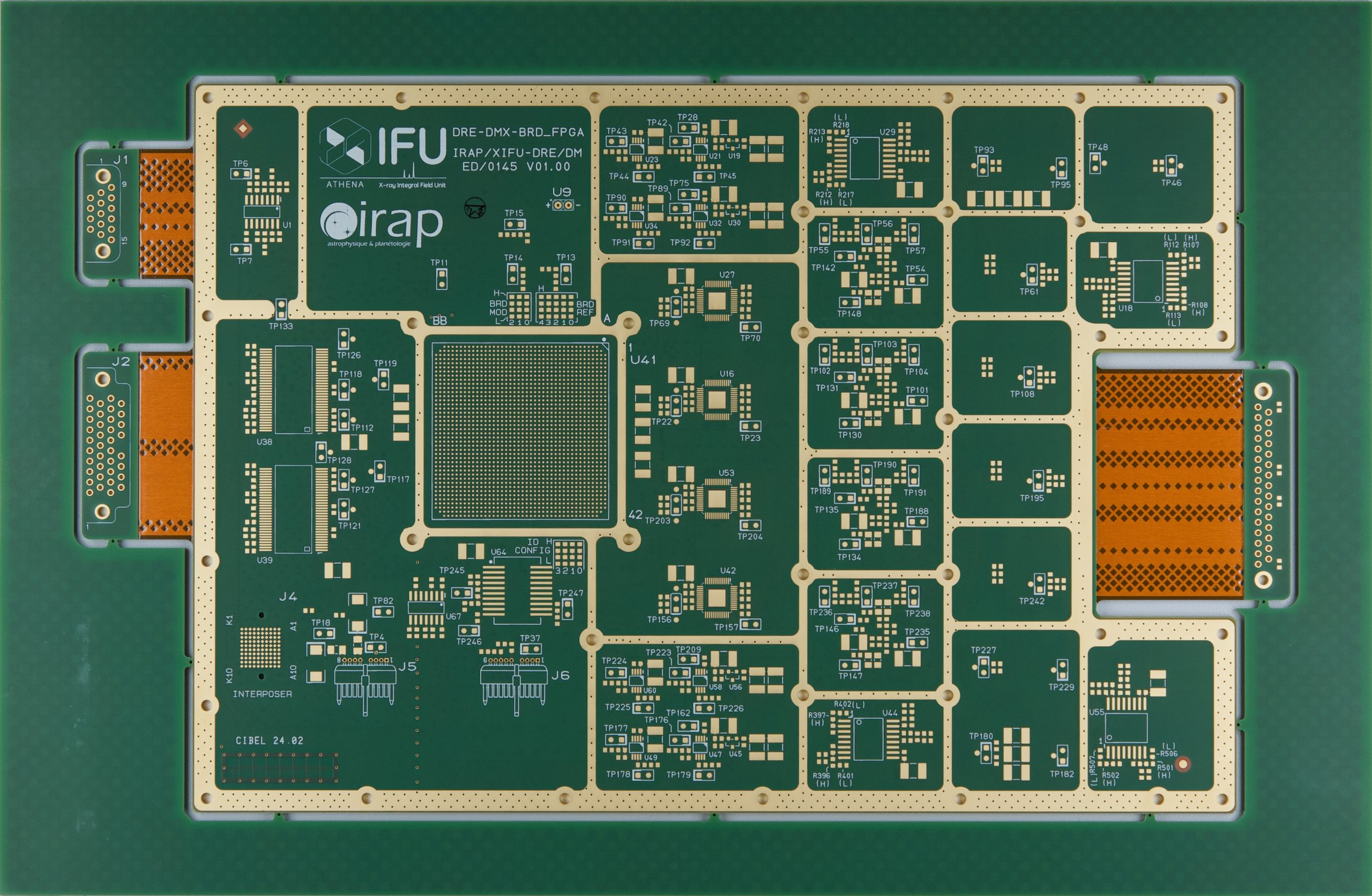
The DRE De-multiplexing (DEMUX) Demonstrator Model (DM) printed circuit board (PCB) arrived at IRAP on January 15. It was designed by the DRE team at IRAP, with CAO-concept handling the layout and CIBEL the manufacturing. The soldering of the components on the board is ongoing.
It consists of a 16-layer rigid and a 4-layer flexible PCB measuring 177 mm x 300 mm. To comply with European Cooperation for Space Standardization (ECSS) design rules, signals are routed through the PCB’s inner layers. Of the 16 layers of the rigid part, only 6 are available for signal routing.
The others are used for ground, power supplies and shielding to ensure a good impedance control of all tracks, thus improving signal integrity. To minimize crosstalk between the detection chains, the PCB is mounted on an aluminum frame, which acts both as a stiffener for the PCB and as an EMC shield between the various sensitive functions. The PCB has been gold-plated at its interface with the stiffener to ensure good electrical and thermal conduction (see photo).
In the DEMUX Demonstrator Model, digital processing is carried out by a new-generation Field-programmable gate array (FPGA): the NanoXplore NG Large. The PCB’s track density is very high. This is particularly true in the FPGA area, which is housed in a 1752-column case with a 1mm pitch. For maximum efficiency, the FPGA power supplies are decoupled directly at the rear of the FPGA.
We will now send the PCB to Matra Electronique, who will solder the components. Testing of the board should begin at the end of March at IRAP.


 Youtube